最近VK3YEが公表したKnobless Wonderという究極のSSBトランシーバーを製作した。コンディションによっては全国とQSOできる事は大きな驚きであった。しかし出力2Wで、最近の電波コンディションの悪さからなかなかQSOが出来ない日もある。。そこでお助けマシーンとしてリニアアンプを作った。

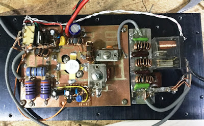
10Wも出ればいいのであるが、部品箱を漁っていたらMRF255が出てきた。一時秋月で格安で放出されていたのでお持ちの方も多いと思う。IMDがあまり良くないとか言われているが、軽く使うには手ごろなFETと思う。電源電圧12Vで使えるところもいい。
回路は作りやすさ、確実性、効率をある程度考慮した。
入力のマッチングはいろいろ難しい。今回は広帯域とし、直結、4:1、1:4と比べてみたところ1:4が一番効率が高かったことから採用した。思ったより入力インピーダンスが高いようだ。
Knobless Wonderが2W出力なので3dBアッテネーターを付けて1Wでドライブするようにした。
出力はLCの狭帯域としている。これは効率を高めるためとKnobless Wonder専用とするためである。アイドリング電流は400mAに設定している。これでピーク35Wまで出力できた。
入力回路も狭帯域にすれば50Wが可能と思われるが、手軽に作れることと10W出力できれば十分と思い、これで完成とした。ピークIdは8A程度であった。
尚、出力にはLPFが必須である。今回シングルFETなので2次高調波をよりカットするため、定K型2段プラス極付き(14MHz)とした。結果としては法令に対しぎりぎりであった。今後製作する場合は定K型3段プラス極付がいいと思う。


Recently I made the ultimate SSB transceiver called Knobless Wonder(VK3YE). On the good condition, It's possible to QSO with the whole in my country(JA). It's was a big surprise. However, with 2W output, there are days when QSO can not be done quite easily due to poor radio condition recently. . So I made a linear amplifier.
I hope to get 10 watts. I found MRF 255 from the parts box.
It is said that IMD is not good, but I think that it is reasonable FET to use lightly. It is also nice to use it with a power supply voltage of 12 V.
The circuit considered ease of manufacture, certainty and efficiency to some extent.
Matching of inputs is difficult. This time it was adopted because it was broadband and compared with direct connection, compared with 4: 1 and 1: 4 where 1: 4 was the most efficient. It seems that input impedance is higher than I expected.
Since Knobless Wonder is 2 W output, it was designed to drive with 1 W with a 3 dB attenuator.
The output is a narrow band of LC. This is to increase efficiency and to be dedicated to Knobless Wonder.
Idling current set 400 mA. With this, we could output up to 35 W peak.
It seems that 50 W is possible if the input circuit is narrowband type LC, but I thought that it would be sufficient if we could produce easily and 10 W could be done, and it was completed with this. The peak Id was about 8 A.
Incidentally, LPF is indispensable for output. Since it is a single FET this time, in order to cut the second harmonic wave further, it is set to constant K type 2 steps plus polar filter(14 MHz). As a result, it was marginal to laws and ordinances. If you plan to make it in the future, I think that it is good to have fixed K type three-stage plus polarity.
Let's enjoy Homebrew.
73's
JA2NKD Ryuu

10Wも出ればいいのであるが、部品箱を漁っていたらMRF255が出てきた。一時秋月で格安で放出されていたのでお持ちの方も多いと思う。IMDがあまり良くないとか言われているが、軽く使うには手ごろなFETと思う。電源電圧12Vで使えるところもいい。
回路は作りやすさ、確実性、効率をある程度考慮した。
入力のマッチングはいろいろ難しい。今回は広帯域とし、直結、4:1、1:4と比べてみたところ1:4が一番効率が高かったことから採用した。思ったより入力インピーダンスが高いようだ。
Knobless Wonderが2W出力なので3dBアッテネーターを付けて1Wでドライブするようにした。
出力はLCの狭帯域としている。これは効率を高めるためとKnobless Wonder専用とするためである。アイドリング電流は400mAに設定している。これでピーク35Wまで出力できた。
入力回路も狭帯域にすれば50Wが可能と思われるが、手軽に作れることと10W出力できれば十分と思い、これで完成とした。ピークIdは8A程度であった。
尚、出力にはLPFが必須である。今回シングルFETなので2次高調波をよりカットするため、定K型2段プラス極付き(14MHz)とした。結果としては法令に対しぎりぎりであった。今後製作する場合は定K型3段プラス極付がいいと思う。


I hope to get 10 watts. I found MRF 255 from the parts box.
It is said that IMD is not good, but I think that it is reasonable FET to use lightly. It is also nice to use it with a power supply voltage of 12 V.
The circuit considered ease of manufacture, certainty and efficiency to some extent.
Matching of inputs is difficult. This time it was adopted because it was broadband and compared with direct connection, compared with 4: 1 and 1: 4 where 1: 4 was the most efficient. It seems that input impedance is higher than I expected.
Since Knobless Wonder is 2 W output, it was designed to drive with 1 W with a 3 dB attenuator.
The output is a narrow band of LC. This is to increase efficiency and to be dedicated to Knobless Wonder.
Idling current set 400 mA. With this, we could output up to 35 W peak.
It seems that 50 W is possible if the input circuit is narrowband type LC, but I thought that it would be sufficient if we could produce easily and 10 W could be done, and it was completed with this. The peak Id was about 8 A.
Incidentally, LPF is indispensable for output. Since it is a single FET this time, in order to cut the second harmonic wave further, it is set to constant K type 2 steps plus polar filter(14 MHz). As a result, it was marginal to laws and ordinances. If you plan to make it in the future, I think that it is good to have fixed K type three-stage plus polarity.
Let's enjoy Homebrew.
73's
JA2NKD Ryuu


